Welcome
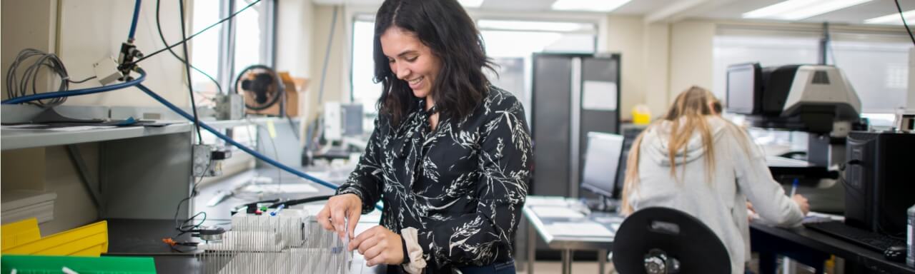
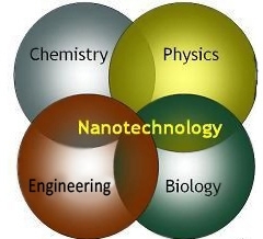
Nanotechnology is expected to reshape everything we know, design, or make. As it goes outside the lab and into production, the associated potential for growth in nanotechnology is limitless. To maintain an edge in a global competition, nanotechnology needs a workforce that is exponentially increasing.
This project contributes to the building of this workforce through building an infrastructure for education in nanotechnology that is sustainable and continuous, with coverage from pre-college, to graduate levels.
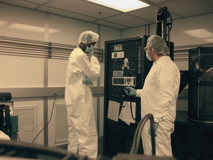
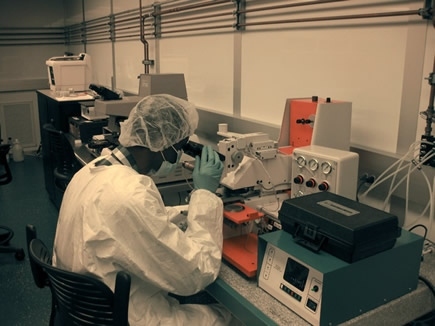
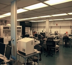
Our Clean Room
The Solid State Electronics Fabrication lab consists of a class 10,000 clean room with approximately 1,000 square feet of work area. The temperature and humidity of the lab are tightly controlled to be 70° ±5° and 42.5% ±3%, respectively. The lab is capable of processes including silicon-based optoelectronics and 3 µm metal-gate NMOS and supports both undergraduate research and education in the areas of solid state devices, integrated circuits, and MEMs/NEMs.
- Atomic Force Microscope (AFM)
- Scanning Electron Microscope (SEM)
- Optical Microscopes
- Four Point Probes
- Semiconductor Parameter Analyzers
- Ellipsometer
- Two Mask Aligners
- Spin-Coating System
- Diffusion Doping Furnace
- Wet and Dry Oxidation Furnace
- Thermal Annealing Furnace
- Thermal Evaporation System
- Wet Chemistry Benches
Courses
Two courses were developed and offered in the area of nanotechnology for engineering and science students. These courses are:
EGR 357 Fundamentals of Nanotechnology
The course introduces students to the field of nanotechnology. Topics include: sizes and scaling laws, characteristics of nanomaterials, growth, fabrication, and measurement techniques for nanostructures, applications in electronics, photonics, mechanics, chemistry, and medicine. In addition, the societal impact and ethical dimensions of nanotechnology will be covered. Laboratory and hands-on activities are integrated in the course lectures.
EGR 457 Nano/Micro Systems Engineering
This is a second course in the nanotechnology sequence. Topics include: micro/nano systems and micro/nano electronics, essential electrical and mechanical concepts, micro/nanosystems design, micro/nano fabrication processes, electrostatic sensing and actuation, piezoresistive sensing and actuation, piezoelectric sensing and actuation, assembly, packaging, and testing of micro/nanosystems. Laboratory includes hands-on projects.
Outreach and Collaborations
As part of the Nanotechnology grant by NSF, multiple educational modules and activities were developed and presented in different venues. Following are some of these activities:
NanoDays
NanoDays took place during the end of March 2011 where middle school students visited GVSU and were given a chance to experience nanotechnology products and understand some of its basics.
Engineering Week at the Museum
Activities similar to “NanoDays” were conducted with a wider and more public audience, during the Engineering Week at the Van Andel Museum in Grand Rapids, MI. March 2011.
STEM Education
A program was developed and implemented to promote STEM education and retention with K–12 school districts in Grand Rapids, MI. The program included the delivery of modules developed by engineering faculty and team-taught with instructors in high school STEM classes. The program is rapidly expanding and more schools are becoming interested in adopting it. A major part of this program relies on nanotechnology modules.
Nanotechnology meets the World
An invited seminar at Central Michigan University was delivered for doctoral students and faculty titled: Nanotechnology meets the World, Oct. 7, 2011. The seminar discussed the challenges in building an undergraduate nanotechnology program as well as the ethical and societal impact of nanotechnology.
Ethics and Societal Impact
Nanotechnology and nano sciences have recently gained tremendous attention and funding, from multiple entities and directions. In the last 10 years the funding for nanotechnology research has increased by orders of magnitude. An important part that has also gained parallel attention is the societal and ethical impact of nanotechnology and the possible consequences of its products and processes on human life and welfare. Click here to learn more about ethics and societal impact.
References and Publications
Jiao H. and N. Barakat, “Balanced Depth and Breadth in a New Interdisciplinary Nanotechnology Course,” Journal of Educational Technology Systems, Vol 40(1), 75 - 87, Baywood Publishing Company, Inc. 2011 – 2012, doi.10.2190/ET.40.1.g, https://baywood.com.
Barakat N. and H. Jiao, “Proposed Strategies for Teaching ethics of Nanotechnology,“ Nanoethics Journal, Springer, Netherlands, Sep. 2010. DOI 10.1007/s11569-010-0100-0.
Jiao H. and N. Barakat, “Incorporation of Hands-on Activities in Learning Nanomaterials,” ASME – IMECE, Nov. 2011, Denver, CO.
Barakat N. and H. Jiao, “Nanotechnology Integration to Enhance Undergraduate Engineering Education,” 1st World Engineering Education Flash Week (WEE2011), September 27-30, 2011, Lisbon, Portugal.
Jiao H. and N. Barakat, “Ion-Sensitive Field Effect Transistor as a PH Sensor,” ChinaNANO, Beijing, China, Sep. 2011.
Barakat N. and H. Jiao, “Development and Implementation of a Comprehensive Nanotechnology Fundamentals Lab for Engineering Students,” ASEE Annual Conference and Exposition, June 26 – 29, Vancouver, BC, Canada, 2011.
Jiao H. and N. Barakat, “Integration of Nanotechnology into Undergraduate Engineering and Science Education,” ASME-IMECE Micro/Nano technology poster forum, Vancouver, BC. Canada, 2010.
Nael Barakat, “The Practical Scope of Nanotechnology Ethics,” Environmental Nano Technologies (ENT) Magazine, issue 3, IANET Association, Rome, Italy, on line: www.entmagazine.com, Dec. 2010.
Contact Us
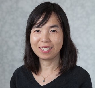
Heidi Jiao
Office Address: 229 Kennedy Hall of Engineering
Phone: (616) 331-6844
Email: [email protected]
Dr. Jiao received her B.S. and M.S. in Electrical Engineering from Nankai University, China and her Ph.D. in Electrical Engineering from Pennsylvania State University. She joined GVSU in 2004 after spending several years working as an engineer and researcher at Motorola, Bell Labs, and AVC Global Services.
Dr. Jiao's teaching and research interests include inorganic/organic solar cell characterization and fabrication, organic light emitting diodes, thin-film transistors, nanomaterials, nanodevices, MEMs sensors, fiber optics, and optical communication networks